Flip-Flops: SR, D, JK, and T
Learning Objectives
By the end of this lesson, you should be able to:
- explain why flip-flops are memory elements;
- distinguish level-sensitive latches from edge-triggered flip-flops;
- use SR, D, JK, and T flip-flop truth tables;
- identify setup time, hold time, clock-to-Q delay, and metastability risk;
- choose a flip-flop type for registers, counters, and control logic;
- debug common wiring, reset, and timing mistakes.
Why Sequential Logic Needs Flip-Flops
Combinational circuits forget immediately. A flip-flop stores one bit, so the circuit can remember a previous state.
The stored value changes only at the active clock edge, except for asynchronous set or reset inputs if the device has them.
Latch Versus Flip-Flop
| Feature | Latch | Flip-flop |
|---|---|---|
| Sensitivity | level-sensitive | edge-triggered |
| Control | enable level | clock edge |
| Output changes | while enable is active | near clock edge only |
| Common use | small gated storage, special timing | registers, counters, FSMs |
Beginners often use the words interchangeably, but timing behavior is different. Most synchronous digital systems are built from edge-triggered flip-flops.
Timing Terms
title "D flip-flop timing terms"
time start=0 end=40 unit=ns divisions=8

CLK: square label="CLK" low=0 high=1 duty=50 cycles=2 unit=logic color=#2563eb
D: step label="D stable before edge" low=0 high=1 at=8 unit=logic color=#16a34a
Q: step label="Q after clock to Q" low=0 high=1 at=22 unit=logic color=#dc2626
marker SETUP at=18 label="setup window"
marker EDGE at=20 label="rising edge"
marker CQ at=22 label="clock to Q"
This waveform is explanatory. Real device values come from the datasheet or FPGA timing report.
Key terms:
| Term | Meaning |
|---|---|
t_setup |
input must be stable before the clock edge |
t_hold |
input must remain stable after the clock edge |
t_CQ |
delay from active clock edge to valid Q |
fmax |
highest safe clock frequency for a timing path |
A simplified maximum clock estimate is:
Tclk >= t_CQ + t_logic + t_setup + t_skew
fmax <= 1 / Tclk
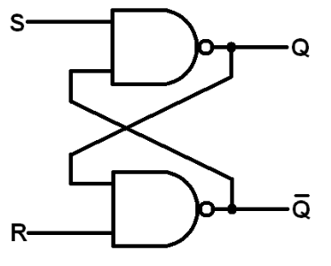
SR Flip-Flop
An SR flip-flop has set and reset inputs.
| S | R | Next Q | Meaning |
|---|---|---|---|
| 0 | 0 | Q | hold |
| 0 | 1 | 0 | reset |
| 1 | 0 | 1 | set |
| 1 | 1 | invalid or forbidden | depends on implementation |
Use SR storage when the design naturally has separate set and reset events. Avoid driving set and reset active at the same time.
D Flip-Flop
A D flip-flop copies input D to output Q on the active clock edge.
| Clock event | D | Next Q |
|---|---|---|
| rising edge | 0 | 0 |
| rising edge | 1 | 1 |
| no active edge | X | Q |
The D flip-flop is the standard storage element for registers, pipelines, finite state machines, and FPGA logic.

Register Example
Four D flip-flops sharing one clock form a 4-bit register.
On each active edge, all four bits update together.
JK Flip-Flop
The JK flip-flop fixes the forbidden SR state by making J=1, K=1 toggle the output.
| J | K | Next Q | Meaning |
|---|---|---|---|
| 0 | 0 | Q | hold |
| 0 | 1 | 0 | reset |
| 1 | 0 | 1 | set |
| 1 | 1 | Q' | toggle |

JK flip-flops are useful in classic counter design and teaching. In FPGA and ASIC RTL, designers more often describe equivalent behavior using D flip-flops because synthesis tools map state to available flip-flop primitives.
T Flip-Flop
A T flip-flop toggles when T=1 and holds when T=0.
| T | Next Q |
|---|---|
| 0 | Q |
| 1 | Q' |
A T flip-flop can be made from a JK flip-flop by tying J=K=T, or from a D flip-flop with:
D = Q xor T

T flip-flops are natural building blocks for counters and frequency dividers.
Asynchronous and Synchronous Reset
Reset brings a stored circuit into a known state.
| Reset type | Behavior | Main risk |
|---|---|---|
| synchronous reset | sampled on a clock edge | reset only works when clock is running |
| asynchronous reset | affects Q immediately | release can violate timing |
In modern synchronous systems, asynchronous reset assertion is common, but deassertion should be synchronized to the receiving clock domain.
Metastability
If a flip-flop input changes too close to the clock edge, the output may briefly settle between valid logic states. This is called metastability.
Metastability cannot be eliminated completely, but it can be made extremely unlikely to affect the system:
- synchronize asynchronous inputs with two or more flip-flops;
- do not use one unsynchronized external signal in many places;
- use proper clock-domain crossing circuits for multi-bit data;
- respect FPGA timing constraints and static timing analysis.
Worked Example: Toggle LED With a D Flip-Flop
Goal: toggle Q on every clock edge.
For a D flip-flop, choose:
D = Q'
Truth table:
| Present Q | D | Next Q |
|---|---|---|
| 0 | 1 | 1 |
| 1 | 0 | 0 |
Every clock edge inverts the output, so the output frequency is half the clock frequency:
fout = fclk / 2
HDL Examples
Verilog D flip-flop with synchronous reset:
always @(posedge clk) begin
  if (rst) begin
    q <= 1'b0;
  end else begin
    q <= d;
  end
end
VHDL D flip-flop with synchronous reset:
process(clk)
begin
  if rising_edge(clk) then
    if rst = '1' then
      q <= '0';
    else
      q <= d;
    end if;
  end if;
end process;
Use nonblocking assignments (<=) for clocked Verilog registers so all flip-flops update together.
Common Mistakes
| Mistake | Symptom | Fix |
|---|---|---|
| Confusing latch and flip-flop | output changes while enable is high | check symbol and timing diagram |
| Violating setup or hold time | intermittent wrong state | slow clock, reduce logic delay, constrain timing |
| Unsynchronized push button | random multiple transitions | debounce and synchronize |
| Releasing async reset near clock edge | some registers start wrong | synchronize reset release |
| Using blocking assignment for sequential Verilog | simulation differs from hardware intent | use nonblocking assignment in clocked blocks |
| Floating set or reset pin | unexpected state changes | tie unused control pins inactive |
Practical Checks
- Confirm the active clock edge.
- Confirm whether reset and set are active-high or active-low.
- Check setup, hold, and clock-to-Q values in the datasheet.
- For FPGA designs, read the timing report rather than guessing
fmax. - Simulate state changes and reset behavior.
- Probe clock, reset, D, and Q together with a logic analyzer when debugging hardware.
Summary
Flip-flops store one bit and make sequential digital systems possible. SR flip-flops teach set/reset behavior, D flip-flops dominate registers and FPGA logic, JK flip-flops add a defined toggle mode, and T flip-flops are ideal for counters. Correct flip-flop design depends as much on timing and reset discipline as on truth tables.
Further Reading
- M. Morris Mano and Michael Ciletti, Digital Design
- Texas Instruments, Designing With Logic
- FPGA vendor timing-closure and clock-domain-crossing guides
- Datasheets for 74HC74, 74HC76, 74HC112, and 74HC393